| CPC H04B 1/04 (2013.01) [H04B 2001/0408 (2013.01)] | 20 Claims |
|
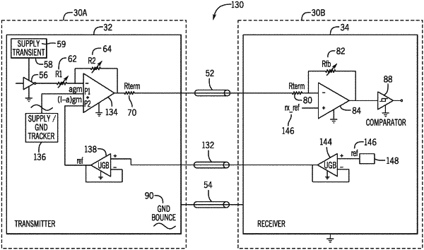
1. An electronic device comprising:
a receiver comprising a first unit gain buffer configured to receive a reference voltage signal;
a transmitter comprising
a second unit gain buffer coupled to the first unit gain buffer of the receiver, the second unit gain buffer being configured to receive the reference voltage signal via the first unit gain buffer,
an amplifier comprising a first positive input configured to receive the reference voltage signal via the first unit gain buffer and the second unit gain buffer,
an offset tracker coupled to a second positive input of the amplifier; and
a connector coupling the first unit gain buffer of the receiver to the second unit gain buffer of the transmitter.
|