| CPC H03K 5/01 (2013.01) [G05F 1/567 (2013.01); H03K 2005/00019 (2013.01)] | 15 Claims |
|
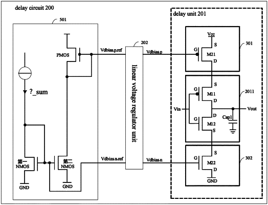
1. A delay circuit, comprising:
a delay unit, wherein the delay unit comprises an inversion unit and a first power supply control unit and a second power supply control unit, wherein the inversion unit receives an input signal and delays the input signal;
a temperature coefficient voltage generating circuit, comprising a first NMOS, a second NMOS and a PMOS; wherein the temperature coefficient voltage generating circuit generates a negative temperature coefficient voltage from the first NMOS and the second NMOS or a positive temperature coefficient voltage from the PMOS; and
a linear voltage regulator unit, coupled to the delay unit, wherein the linear voltage regulator unit inputs the positive temperature coefficient voltage and outputs a first power supply control signal according to the positive temperature coefficient voltage; and/or the linear voltage regulator unit inputs the negative temperature coefficient voltage and outputs a second power supply control signal according to the negative temperature coefficient voltage;
wherein the inversion unit receives a power supply voltage based on the first power supply control signal from the first power supply control unit, and wherein the inversion unit receives a ground voltage based on the second power supply control signal from the second power supply control unit.
|