| CPC H03K 19/018521 (2013.01) [H03K 3/037 (2013.01)] | 10 Claims |
|
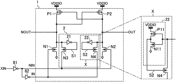
1. A level shift circuit, comprising:
an input node receiving an input signal transitioning between a first power supply and a second power supply lower in potential than the first power supply;
an inverted input node receiving an inverted input signal inverted from the input signal;
a first n-type transistor having a gate connected to the input node, a source connected to the second power supply or the inverted input node, and a drain connected to an inverted output node;
a first p-type transistor having a drain connected to the inverted output node, a source connected to a third power supply higher in potential than the first power supply, and a gate connected to an output node;
a second n-type transistor having a gate connected to the inverted input node, a source connected to the second power supply or the input node, and a drain connected to the output node;
a second p-type transistor having a drain connected to the output node, a source connected to the third power supply, and a gate connected to the inverted output node;
a third n-type transistor having a source connected to the inverted input node and a drain connected to the inverted output node;
a first inverter having an input connected to the inverted output node and an output connected to a gate of the third n-type transistor;
a fourth n-type transistor having a source connected to the input node and a drain connected to the output node; and
a second inverter having an input connected to the output node and an output connected to a gate of the fourth n-type transistor.
|