| CPC H03K 19/00315 (2013.01) [H03K 19/20 (2013.01)] | 20 Claims |
|
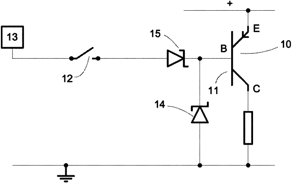
1. A circuit comprising:
a transistor;
a signal source;
a base of the transistor being switchably connectable to the signal source;
a first diode connected between the base of the transistor, and a reference voltage;
wherein the circuit is arranged such that when the signal source is not connected to the base of the transistor, a voltage applied at an emitter of the transistor causes a current flow through the base of the transistor and through the first diode such that the transistor is in an ON state;
the impedance of the signal source is lower than the impedance of the transistor through the emitter and base;
the first diode provides a current limiting function such that when the signal source is connected to the base of the transistor, current flow through the base reduces such that the transistor switches to an OFF state; and in which
the circuit comprises a second diode, the second diode comprised from a semiconductor region that provides the base of the transistor and a further semiconductor region in direct contact with the semiconductor region that provides the base of the transistor; and in which the signal source is connectable to the base of the transistor through the second diode.
|