| CPC H03H 9/059 (2013.01) [H01L 24/03 (2013.01); H01L 24/05 (2013.01); H01L 24/11 (2013.01); H01L 24/13 (2013.01); H03H 3/08 (2013.01); H03H 9/64 (2013.01); H10N 30/06 (2023.02); H10N 30/875 (2023.02); H10N 30/877 (2023.02); H01L 2224/0401 (2013.01); H01L 2224/05084 (2013.01); H01L 2224/05124 (2013.01); H01L 2224/05147 (2013.01); H01L 2224/05166 (2013.01); H01L 2224/05171 (2013.01); H01L 2224/05184 (2013.01); H01L 2224/05655 (2013.01); H01L 2924/0132 (2013.01)] | 30 Claims |
|
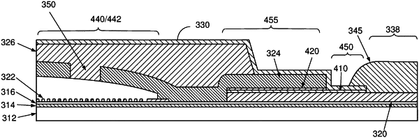
1. A chip, comprising:
a pad;
a first passivation layer, wherein a first portion of the first passivation layer extends over a first portion of the pad;
a first metal layer between the first portion of the pad and the first portion of the first passivation layer; and
an under bump metallization (UBM) electrically coupled to a second portion of the pad, wherein a first portion of the UBM is over the second portion of the pad.
|