| CPC H02M 7/493 (2013.01) [H02M 1/0058 (2021.05); H02M 1/325 (2021.05); H02M 7/003 (2013.01); H02M 7/217 (2013.01); H02M 7/4835 (2021.05); H02M 7/5395 (2013.01); H02M 1/007 (2021.05); H02M 1/0054 (2021.05); H02M 1/327 (2021.05); H02M 3/33573 (2021.05); H02M 7/4807 (2013.01)] | 14 Claims |
|
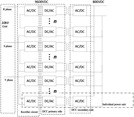
1. A Pulse Width Modulation (PWM) method for a Cascaded H-bridge (CHB) converter, wherein each phase of the CHB converter connected to a three-phase AC power supply is provided with n CHB rectifier circuits, where n is greater than 1, and each CHB rectifier circuit is provided with a first AC input terminal, a second AC input terminal, a positive DC output terminal, a negative DC output terminal, four power transistors connected to form a H-bridge structure, and a DC bus capacitor,
the PWM method comprising the steps of:
S1, generating a pair of sinusoidal signals with a phase difference of 180 degrees as a first reference waveform and a second reference waveform, and generating n carrier signals having sequentially decreasing levels and equal amplitudes to correspond to the n H-bridge rectifier circuits, respectively, wherein the levels of the n carrier signals are cascaded to fill the amplitude of a unipolar voltage half cycle of the reference waveform; and
S2, determining PWM signals for controlling the corresponding H-bridge rectifier circuits based on each reference waveform and each of the n carrier signals, and controlling, by n groups of the PWM signals, the power transistors in the n H-bridge rectifier circuits to switch on and off.
|