| CPC H02M 3/33569 (2013.01) [H02M 1/327 (2021.05); H02M 7/003 (2013.01); H02M 7/537 (2013.01); H02M 7/5387 (2013.01); H02M 7/53871 (2013.01)] | 17 Claims |
|
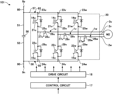
1. A power converter comprising:
a capacitor;
a substrate on which a plurality of switching elements for power conversion are mounted;
a cooler for cooling the plurality of switching elements;
a housing that accommodates the capacitor, the substrate, and the cooler;
a power connector exposed from the housing;
an output connector exposed from the housing; and
a plurality of lines that include
a plurality of power lines each electrically connected to the capacitor, given switching elements, and the power connector, and
a plurality of output lines each electrically connected to a given switching element and the output connector,
wherein at least one among the plurality of lines is a line that includes a conductive pattern formed on the substrate.
|