| CPC H02M 3/073 (2013.01) [G05F 3/205 (2013.01); H02M 3/072 (2021.05)] | 5 Claims |
|
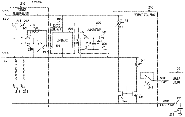
1. A DC/DC converter, comprising:
a charge pump configured to generate a specific output voltage from a specific DC power supply;
a clock generator configured to output a clock for operating the charge pump;
a voltage monitoring unit configured to:
monitor the specific output voltage of the charge pump;
and
control the clock output from the clock generator such that the specific output voltage is maintained within a specific range;
compare the specific output voltage with one of a first potential or a second potential;
output a control signal that enables output of the clock when the specific output voltage goes beyond one of the first potential or the second potential:
compare the specific output voltage with the first potential when the control signal indicates invalidity of the clock;
compare the specific output voltage with the second potential when the control signal indicates validity of the clock; and
compare the specific output voltage with the second potential when a specific forced signal is input even in a case where the control signal indicates invalidity of the clock; and
a voltage regulator configured to generate a bias voltage from the specific output voltage of the charge pump.
|