| CPC H02H 9/046 (2013.01) [H01L 27/0266 (2013.01)] | 19 Claims |
|
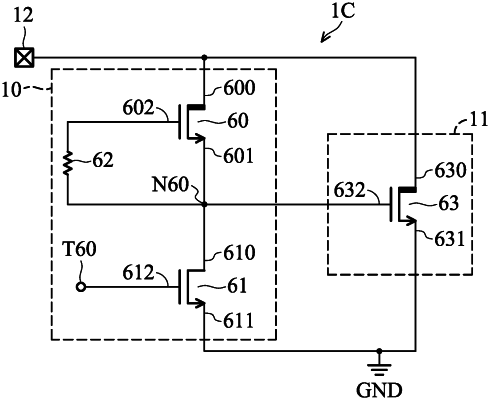
1. A protection circuit, coupled to a bounding pad, comprising:
a trigger circuit comprising a first transistor of a first conductivity type and a second transistor of the first conductivity type coupled in series between the bonding pad and a ground terminal further comprising a resistor, wherein the trigger circuit detects whether a transient event occurs on the bonding pad; and
a discharge circuit, coupled between the bonding pad and the ground terminal and controlled by the trigger circuit,
wherein, in response to the transient event occurring on the bonding pad, the trigger circuit generates a trigger voltage to trigger the discharge circuit to provide a discharge path between the bonding pad and the ground terminal, and
wherein:
the first transistor comprises a first electrode terminal coupled to the bonding pad, a second electrode terminal coupled to a first node, and a control electrode terminal,
the second transistor is coupled between the first node and the ground terminal, and
the resistor is coupled between the control electrode terminal of the first transistor and the discharge circuit.
|