| CPC H01S 5/18394 (2013.01) [H01S 5/18352 (2013.01); H01S 5/423 (2013.01)] | 14 Claims |
|
1. A surface emitting laser device, comprising:
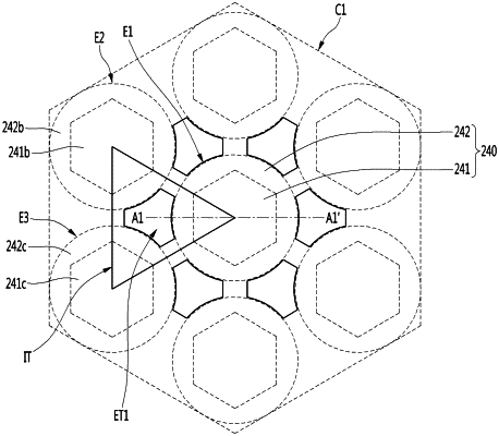
a first emitter including a first polygonal shaped aperture and a first circular shaped insulating region;
a second emitter including a second polygonal shaped aperture and a second circular shaped insulating region and disposed adjacent to the first emitter;
a third emitter including a third polygonal shaped aperture and a third circular shaped insulating region and disposed adjacent to the first emitter and the second emitter, and the third emitter disposed on a first side of a first virtual line connecting a center of the first polygonal shaped aperture and a center of the second polygonal shaped aperture; and
a first trench region disposed between the first emitter, the second emitter and the third emitter and forming sidewalls of the first emitter, the second emitter and the third emitter,
wherein the first trench region is disposed inside a virtual triangle connecting the center and two corners of the first polygonal shaped aperture of the first emitter, the center and two corners of the second polygonal shaped aperture of the second emitter, and a center and two corners of the third polygonal shaped aperture of the third emitter,
wherein the first trench region includes a first round region forming a first portion of a sidewall of the insulating region of the first emitter, a second round region forming a first portion of a sidewall of the insulating region of the second emitter, and a third round region forming a first portion of a sidewall of the insulating region of the third emitter,
wherein the first, second and third round regions of the first trench respectively face sides of the first, second and third polygonal shaped apertures and are disposed inside the virtual triangle, and
wherein a center angle of a sector having the first round region as an arc is 25 to 45°.
|