| CPC H01R 12/62 (2013.01) [G06F 3/04164 (2019.05); H01R 43/0207 (2013.01); H05K 1/0277 (2013.01); H05K 1/111 (2013.01); H05K 1/142 (2013.01)] | 19 Claims |
|
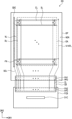
1. A display device comprising:
a display panel comprising a substrate and a panel pad which is on the substrate;
a circuit board which provides a driving signal; and
a connection board which connects the display panel to the circuit board, the connection board comprising:
a flexible substrate having a first edge and a second edge which are opposite to each other, and
a connection line which is on the flexible substrate and extends from the first edge to the second edge, the connection line comprising:
a first end portion which is on the first edge of the flexible substrate and is between the substrate of the display panel and the flexible substrate of the connection board, along a thickness direction of the display device, and
the first end portion of the connection line is directly connected to the panel pad of the display panel by an ultrasonic vibration bond.
|