| CPC H01Q 3/36 (2013.01) [H01Q 1/38 (2013.01); H01Q 1/50 (2013.01)] | 17 Claims |
|
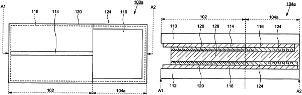
1. An antenna device comprising:
a strip conductor layer;
a radiation conductor layer continuous from the strip conductor layer;
a ground conductor layer facing the strip conductor layer and the radiation conductor layer;
a liquid crystal layer between the strip conductor layer and the ground conductor layer, and the radiation conductor layer and the ground conductor layer; and
an alignment film between the strip conductor layer and the liquid crystal layer, and the radiation conductor layer and the liquid crystal layer,
wherein the alignment film includes a first region overlapping the strip conductor layer and a second region overlapping the radiation conductor layer, and the alignment state of liquid crystal molecules of the liquid crystal layer in the first region is different from the alignment state of liquid crystal molecules of the liquid crystal layer in the second region.
|