| CPC H01M 10/0583 (2013.01) [H01M 10/0431 (2013.01); H01M 10/0525 (2013.01); H01M 50/105 (2021.01); H01M 50/211 (2021.01); H01M 50/247 (2021.01); H01M 50/466 (2021.01)] | 8 Claims |
|
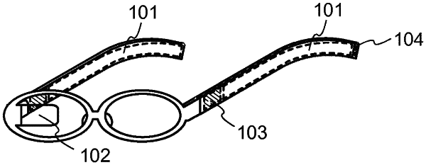
1. An electronic device comprising a secondary battery,
wherein the secondary battery includes a first positive electrode current collector, a second positive electrode current collector, a first negative electrode current collector, and a second negative electrode current collector,
wherein the first positive electrode current collector and the second positive electrode current collector are electrically connected to each other at a first side of the secondary battery,
wherein the first negative electrode current collector and the second negative electrode current collector are electrically connected to each other at a second side of the secondary battery,
wherein the secondary battery includes a curved portion,
wherein the curved portion is closer to the second side than a midpoint of a long side of the secondary battery,
wherein the first negative electrode current collector is provided with a negative electrode active material layer on a first surface and is not provided with a negative electrode active material layer on an entirety of a second surface,
wherein the second negative electrode current collector is not provided with a negative electrode active material layer on an entirety of a first surface and is provided with a negative electrode active material layer on a second surface,
wherein the second surface of the first negative electrode current collector and the first surface of the second negative electrode current collector are in direct contact with each other, and
wherein the entirety of the second surface of the first negative electrode current collector and the entirety of the first surface of the second negative electrode current collector are regions that are not coated with the negative electrode active material layers.
|