| CPC H01L 33/62 (2013.01) [H01L 33/005 (2013.01); H01L 33/10 (2013.01); H01L 2933/0066 (2013.01)] | 15 Claims |
|
1. A display device, comprising:
a substrate;
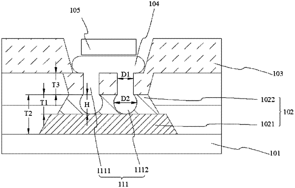
a conductive layer disposed on the substrate, the conductive layer comprising a plurality of sub-conductive layers stacked in sequence; and
a reflective layer disposed on the conductive layer;
wherein a plurality of flask-shaped holes are disposed in the reflective layer and part of the conductive layer,
each of the flask-shaped holes comprises an arc-shaped bottom portion and a cylindrical portion connected to the arc-shaped bottom portion, the arc-shaped bottom portion is disposed in the conductive layer, and the cylindrical portion penetrates the reflective layer, and
a depth of the arc-shaped bottom portion is greater than half of a thickness of an uppermost one of the sub-conductive layers and less than a thickness of the conductive layer.
|