| CPC H01L 33/382 (2013.01) [H01L 33/00 (2013.01); H01L 33/10 (2013.01); H01L 33/24 (2013.01); H01L 33/385 (2013.01); H01L 33/387 (2013.01); H01L 33/42 (2013.01); H01L 33/46 (2013.01); H01L 33/62 (2013.01); H01L 33/0012 (2013.01); H01L 33/02 (2013.01); H01L 33/08 (2013.01); H01L 33/22 (2013.01); H01L 33/38 (2013.01); H01L 33/405 (2013.01); H01L 33/44 (2013.01); H01L 2224/48091 (2013.01); H01L 2224/73265 (2013.01)] | 15 Claims |
|
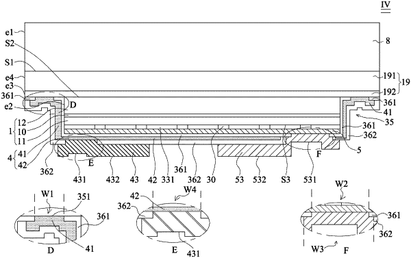
1. A semiconductor light-emitting device, comprising:
a substrate;
a semiconductor stack formed on the substrate and comprising a first semiconductor layer and a second semiconductor layer, wherein the second semiconductor layer is closer to the substrate than the first semiconductor layer is to the substrate;
a first reflective layer formed on the first semiconductor layer and comprising a plurality of vias, wherein the first reflective layer comprises a material having a refractive index lower than that of the group III-V semiconductor;
a plurality of contact structures respectively filled in the plurality of vias and electrically connected to the first semiconductor layer, wherein the plurality of contact structures is surrounded by the first reflective layer;
a second reflective layer comprising metal material formed on the first reflective layer and contacting the plurality of contact structures;
a plurality of conductive vias surrounded by the semiconductor stack;
a connecting layer formed in the plurality of conductive vias and electrically connected to the second semiconductor layer;
a second insulating layer formed on the connecting layer and comprising a third opening on the plurality contact structures and a fourth opening on the plurality contact structures;
a first pad portion formed on the fourth opening and electrically connected to the second semiconductor layer;
a second pad portion formed on the third opening and electrically connected to the first semiconductor layer, wherein a shortest distance between two of the plurality of conductive vias is larger than a shortest distance between the first pad portion and the second pad portion; and
wherein the first pad portion comprises a first face and a second face protruding the first face, a height is formed between the first face and the second face, and is larger than or equal to a thickness of the second insulating layer in a cross-sectional view of the semiconductor light-emitting device.
|