US 11,894,486 B2
Method for manufacturing semiconductor device
Shunpei Yamazaki, Tokyo (JP); Miyuki Hosoba, Kanagawa (JP); and Suzunosuke Hiraishi, Kanagawa (JP)
Assigned to Semiconductor Energy Laboratory Co., Ltd., Atsugi (JP)
Filed by Semiconductor Energy Laboratory Co., Ltd., Atsugi (JP)
Filed on Nov. 1, 2022, as Appl. No. 17/978,269.
Application 17/978,269 is a continuation of application No. 16/196,091, filed on Nov. 20, 2018, abandoned.
Application 16/196,091 is a continuation of application No. 15/685,005, filed on Aug. 24, 2017, granted, now 10,396,236, issued on Aug. 27, 2019.
Application 15/685,005 is a continuation of application No. 13/899,736, filed on May 22, 2013, granted, now 9,748,436, issued on Aug. 29, 2017.
Application 13/899,736 is a continuation of application No. 12/954,181, filed on Nov. 24, 2010, granted, now 8,471,256, issued on Jun. 25, 2013.
Claims priority of application No. 2009-270784 (JP), filed on Nov. 27, 2009.
Prior Publication US 2023/0057493 A1, Feb. 23, 2023
Int. Cl. H01L 33/00 (2010.01); H01L 27/12 (2006.01); H01L 29/786 (2006.01); G02F 1/1368 (2006.01); H10K 59/121 (2023.01)
CPC H01L 33/0041 (2013.01) [H01L 27/124 (2013.01); H01L 27/1225 (2013.01); H01L 29/7869 (2013.01); G02F 1/1368 (2013.01); H01L 2924/0002 (2013.01); H10K 59/1213 (2023.02)] 6 Claims
OG exemplary drawing
 
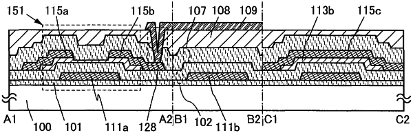
1. A method of manufacturing a semiconductor device, comprising:
forming a gate electrode including copper over a substrate;
forming a first insulating layer over the gate electrode;
forming an oxide semiconductor layer over the first insulating layer;
performing a first heat treatment at a temperature equal to or higher than 350° C. and equal to or lower than 700° C.;
forming a source electrode and a drain electrode after the first heat treatment;
forming a second insulating layer over and in contact with the source electrode, the drain electrode and a portion of the oxide semiconductor layer; and
performing a second heat treatment after forming the second insulating layer,
wherein the first insulating layer includes silicon nitride and silicon oxide over the silicon nitride, and
wherein the second insulating layer includes silicon oxide and silicon nitride over the silicon oxide.