| CPC H01L 31/1856 (2013.01) [H01L 31/03044 (2013.01); H01L 31/1896 (2013.01)] | 3 Claims |
|
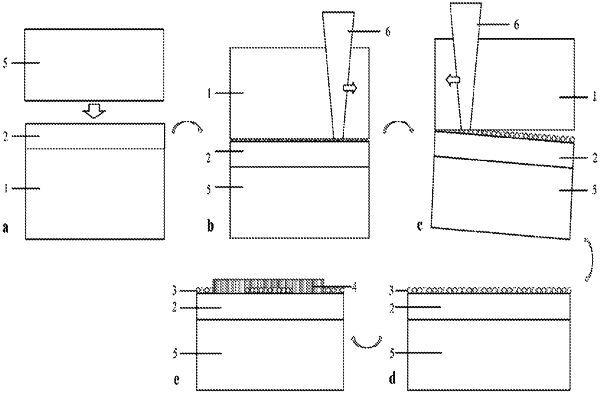
1. A laser rapid fabrication method for flexible gallium nitride (GaN) photodetector, comprising the following steps:
step (1) providing a GaN epitaxial wafer which comprises a GaN film and a rigid transparent substrate, bonding a flexible substrate to the GaN film to obtain a rigid transparent substrate/GaN film/flexible substrate structure;
step (2) placing the rigid transparent substrate/GaN film/flexible substrate structure on a processing table with a fixed height below a light outlet, providing a laser beam incident from a side of the rigid transparent substrate, adjusting a focus of the laser beam so that a focal plane of the laser beam is located within a range of 0.2 mm from an interface between the rigid transparent substrate and the GaN film in the rigid transparent substrate/GaN film/flexible substrate structure described in step (1), a spot size l0 of the laser beam is 5-100 μm;
step (3) selecting laser wavelength in the range of 250-1200 nm, and selecting a ultrafast laser with pulse width less than or equal to 10−12 s, setting laser pulse frequency f0 to 200 kHz-1 MHz; selecting low single pulse energy I1 of 0.1-1 μJ, low laser scanning speed v1 and small scanning spacing d1 as processing parameters, scanning the rigid transparent substrate/GaN film/flexible substrate structure obtained in step (1) with the laser beam, the scanning starts from an edge of the rigid transparent substrate/GaN film/ flexible substrate structure and proceeds along a scan path, where l0, f0, v1 and d1 meet the requirement of:
 upon scanning, GaN at the interface between the GaN film and the rigid transparent substrate is decomposed and Ga metal nanoparticles are precipitated at the interface by irradiation of the laser beam to obtain a rigid transparent substrate/GaN film/flexible substrate structure having Ga metal nanoparticles;
step (4) selecting the same pulse width, the same laser wavelength and the same laser pulse frequency as those in step (3); selecting high single pulse energy I2 of 1-2 μJ, high laser scanning speed v2 and large scanning spacing d2 as processing parameters, scanning the rigid transparent substrate/GaN film/flexible substrate structure having Ga metal nanoparticles with the laser beam in a reverse direction along the scan path in step (3), where l0, f0, v2 and d2 meet the requirement of:
 separating the GaN film and the rigid transparent substrate from the interface between the GaN film and the rigid transparent substrate;
step (5) removing the rigid transparent substrate separated in step (4) to obtain a Ga metal nanoparticle/GaN film/flexible substrate structure;
step (6) forming interdigital electrodes on a surface of the Ga metal nanoparticles in the Ga metal nanoparticle/GaN film/flexible substrate structure obtained in step (5) to obtain the flexible GaN photodetector.
|