| CPC H01L 31/109 (2013.01) [G06F 3/0412 (2013.01); H01L 27/14603 (2013.01); H01L 27/14607 (2013.01); H01L 27/14612 (2013.01); H01L 27/14678 (2013.01); H01L 31/0264 (2013.01); H01L 31/022408 (2013.01); H01L 31/0336 (2013.01); H01L 31/18 (2013.01); H10K 59/60 (2023.02)] | 8 Claims |
|
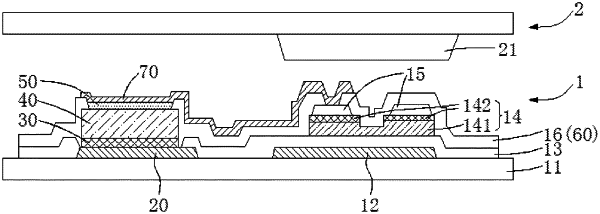
1. A display device, comprising a photosensitive element and pixel units, wherein the photosensitive element is located between two adjacent ones of the pixel units and comprises:
a first base;
a first electrode arranged on the first base;
an N-type doped silicon layer arranged on the first electrode;
an undoped silicon layer arranged on the N-type doped silicon layer;
a molybdenum oxide layer arranged on the undoped silicon layer;
a dielectric layer arranged on the molybdenum oxide layer and the first base, wherein the dielectric layer is provided with a first opening to expose the molybdenum oxide layer; and
a second electrode arranged on the dielectric layer and the molybdenum oxide layer, wherein the second electrode contacts the molybdenum oxide layer through the first opening; and
wherein the display device comprises a first substrate and a second substrate arranged opposite to each other, and the first substrate comprises:
the first base;
a first electrode layer arranged on the first base, the first electrode layer comprising the first electrode and a gate electrode spaced from the first electrode;
a gate insulating layer arranged on the first electrode layer, wherein the gate insulating layer exposes the first electrode;
the N-type doped silicon layer, the undoped silicon layer, and the molybdenum oxide layer arranged on the first electrode in sequence;
an active layer arranged at a position where the gate insulating layer faces the gate electrode, wherein the active layer comprises an undoped part and a doped part;
a source electrode and a drain electrode arranged on the active layer, wherein each of the source electrode and the drain electrode is in contact with the doped part;
the dielectric layer arranged on the molybdenum oxide layer, the source electrode, and the drain electrode, wherein the dielectric layer exposes the molybdenum oxide layer and the drain electrode; and
the second electrode arranged on the dielectric layer, wherein one end of the second electrode is in contact with the molybdenum oxide layer, and another end of the second electrode is in contact with the drain electrode.
|