| CPC H01L 31/035281 (2013.01) [H01L 31/028 (2013.01); H01L 31/02167 (2013.01); H01L 31/02168 (2013.01); H01L 31/0304 (2013.01); H01L 31/03046 (2013.01); H01L 31/03762 (2013.01); H01L 31/0445 (2014.12); H01L 31/0547 (2014.12); H01L 31/1804 (2013.01); H01L 31/184 (2013.01); H01L 31/1808 (2013.01); H01L 31/1844 (2013.01); H01L 31/1868 (2013.01); H01L 31/202 (2013.01)] | 10 Claims |

|
1. A transparent semiconductor substrate comprising:
a semiconductor substrate including a first surface and a second surface opposite to the first surface, wherein the first surface is parallel to the second surface, wherein the semiconductor substrate includes crystalline silicon (c-Si), germanium (Ge), gallium arsenide (GaAs), gallium arsenide Phosphide (GaAsP), amorphous silicon (a-Si), or a combination thereof; and
a plurality of through-holes, each through-hole penetrating the semiconductor substrate,
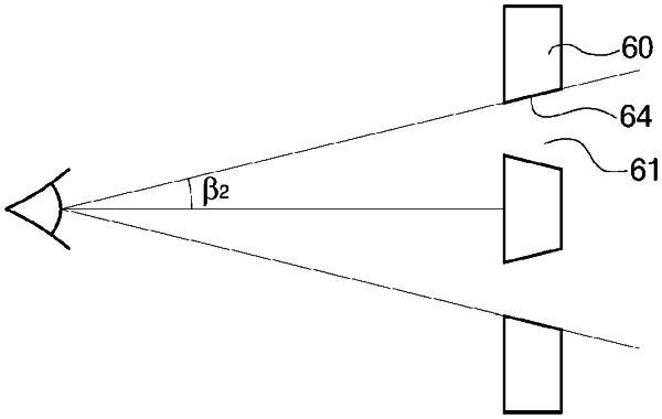
wherein each through-hole includes an inclined portion having a first and a second inclined portions with respect to the first surface and second surface, the first inclined portion forming a first acute angle θ1 with respect to the first surface and the second inclined portion forming a second acute angle θ2 with respect to the first surface, wherein the first acute angle θ1 is same as the second acute angle θ2, wherein a diameter of each through-hole increases from the first surface to the second surface, wherein the diameter of each through-hole at the first surface is smaller than the diameter of each through-hole at the second surface, wherein the first surface is positioned to receive incident light,
wherein the inclined portion is formed with a coating layer which is a light-reflecting layer or an anti-reflection layer,
wherein a total area of the plurality of through-holes on the first surface is smaller than a total area of the plurality of through-holes on the second surface, the total area of the plurality of through-holes on the first surface is formed 5% to 95% of a total area of the semiconductor substrate, and the total area of the plurality of through-holes on the second surface is formed 6% to 96% of the total area of the semiconductor substrate,
wherein a distance between adjacent through holes on the first surface is equal to or less than 200 μm,
wherein the diameter of each through-hole on the first surface is defined so that a haze value calculated by Equation 1 below is less than 1%,
H(%)=Td/Tt×100 <Equation 1>
where Td is diffuse transmittance and Tt is total transmittance.
|