| CPC H01L 31/02322 (2013.01) [B81B 7/0077 (2013.01); B81C 1/00269 (2013.01); H01L 31/02325 (2013.01); B81B 2201/0285 (2013.01); B81B 2201/0292 (2013.01); B81C 2203/0109 (2013.01); B81C 2203/032 (2013.01)] | 10 Claims |
|
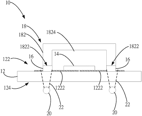
1. A method for manufacturing a sensing module, comprising:
providing a substrate;
disposing or forming a sensor on a first surface of the substrate;
disposing at least one colloid on the first surface to surround the sensor;
disposing an optical conversion element on the substrate and bonding at least one colloid with a lower edge of the optical conversion element, forming a hermetic chamber between the optical conversion element and the substrate; and
using a light source to irradiate a second surface of the substrate, making a plurality of light rays of the light source penetrates the substrate to irradiate and solidify the at least one colloid;
wherein a material of the substrate is selected from a group of acrylic, glass, sapphire, and silicon; the material of optical conversion element is selected from a group of silicon, germanium and zinc sulfide.
|