| CPC H01L 31/02161 (2013.01) [H01L 27/1443 (2013.01); H01L 27/14678 (2013.01); H01L 27/14612 (2013.01); H01L 27/14623 (2013.01); H01L 27/14625 (2013.01)] | 12 Claims |
|
1. An optical sensor, comprising:
a substrate;
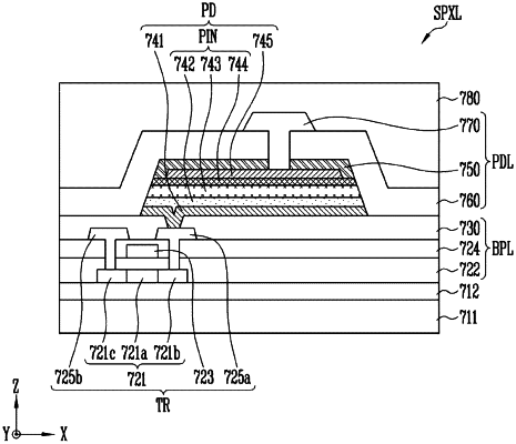
a photoelectric element disposed on the substrate, wherein the photoelectric element includes a first electrode, an intermediate layer disposed on the first electrode, and a second electrode disposed on the intermediate layer;
a barrier layer disposed on the second electrode;
an insulating layer that covers the photoelectric element and the barrier layer,
a bias electrode disposed on the insulating layer and electrically connected to the second electrode; and
an organic planarization layer disposed directly on and above the bias electrode and on and above the insulating layer, and that has a flat upper surface,
wherein the barrier layer is spaced apart from the first electrode.
|