| CPC H01L 29/882 (2013.01) [H01L 29/045 (2013.01); H01L 29/0657 (2013.01); H01L 29/1606 (2013.01); H01L 29/24 (2013.01); H01L 29/267 (2013.01); H01L 29/417 (2013.01); H01L 29/66977 (2013.01); H01L 31/032 (2013.01)] | 32 Claims |
|
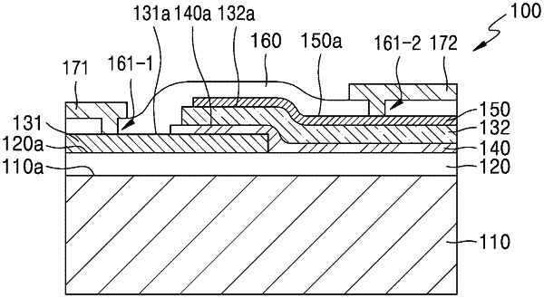
1. A resonant tunneling device, comprising:
a first two-dimensional semiconductor layer including a first two-dimensional semiconductor material;
a first insulating layer on the first two-dimensional semiconductor layer; and
a second two-dimensional semiconductor layer on the first insulating layer, the second two-dimensional semiconductor layer including a second two-dimensional semiconductor material of a same kind as the first two-dimensional semiconductor material,
wherein a crystal lattice of the first two-dimensional semiconductor material and a crystal lattice of the second two-dimensional semiconductor material are aligned with each other, such that the first two-dimensional semiconductor material and the second two-dimensional semiconductor material are configured to have respective energy bands that are aligned with each other.
|