| CPC H01L 29/8725 (2013.01) [H01L 29/24 (2013.01); H01L 29/36 (2013.01); H01L 29/407 (2013.01); H01L 29/66969 (2013.01)] | 22 Claims |
|
1. A Group III trioxide semiconductor device comprising:
a first electrically conductive contact layer;
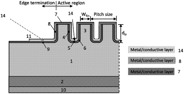
an n-type group III trioxide single crystal material layer disposed electrically operatively in contact with the first electrically conductive contact layer, the n-type group III trioxide single crystal material layer having a first distal surface disposed away from the first electrically conductive contact layer, at least two upstanding channels, each upstanding channel having a distal top surface and sidewalls extending between the distal top surface and the first distal surface of the n-type group III trioxide single crystal material layer; a height of at least one upstanding channel being equal to a distance between the distal top surface and the first distal surface; said each upstanding channel being entirely separated from another upstanding channel by a trench; the first distal surface being disposed between the first electrically conductive contact layer and the distal top surface; said first distal surface being located below the distal top surface and above the first electrically conductive contact layer, bottom corners of each trench being curved; a doping concentration of the n-type group III trioxide single crystal material layer being one of a varying doping concentration, the varying doping concentration having a largest value and a smallest value according to a predetermined configuration, and a predetermined doping concentration;
a dielectric layer deposited over the first distal surface, over sidewalls of each upstanding channel, and over a bottom surface of each trench of the n-type group III trioxide single crystal material layer;
a second electrically conductive layer deposited over the dielectric layer on the sidewalls of each upstanding channel;
a third electrically conductive layer deposited over the dielectric layer on the bottom surface of each trench, and over a portion of the dielectric layer on the first distal surface; the third electrically conductive layer, being disposed, over the portion of the dielectric layer on the first distal surface, a predetermined distance away from a vertical edge surface of the group III trioxide semiconductor device; the third electrically conductive layer being disposed a predetermined distance away from a vertical edge surface of the group III trioxide semiconductor device forms a field-plate for edge termination; the vertical edge surface extending from the first electrically conductive contact layer to the first distal surface; the first distal surface being in contact with the vertical edge surface; the third electrically conductive layer being in electrical contact with the second electrically conductive layer; and
a fourth electrically conductive layer deposited over the distal top surface of each upstanding channel; the fourth electrically conductive layer being in electrical contact with the second electrically conductive layer; wherein there are no p-type regions in the Group III trioxide semiconductor device; wherein the Group III trioxide semiconductor device has breakdown voltage of more than 1200 volts and an on resistance of less than 20 mΩ·cm2; from the breakdown voltage of more than 1200 volts and an on resistance of less than 20 mΩ·cm2 of the Group III trioxide semiconductor device, a value of a Baliga Figure of Merit is obtained for the Group III trioxide semiconductor device; wherein the group III trioxide semiconductor device is a barrier Schottky diode.
|