US 11,894,467 B2
Doped metal oxide semiconductor and thin-film transistor made therefrom and its application
Miao Xu, Guangzhou (CN); Hua Xu, Guangzhou (CN); Weijing Wu, Guangzhou (CN); Weifeng Chen, Guangzhou (CN); Lei Wang, Guangzhou (CN); and Junbiao Peng, Guangzhou (CN)
Assigned to South China University of Technology, Guangzhou (CN)
Filed by South China University of Technology, Guangzhou (CN)
Filed on Nov. 8, 2019, as Appl. No. 16/678,116.
Claims priority of application No. 201910896373.4 (CN), filed on Sep. 18, 2019.
Prior Publication US 2021/0083124 A1, Mar. 18, 2021
Int. Cl. H01L 29/786 (2006.01); H01L 29/24 (2006.01); H01L 29/423 (2006.01); H01L 29/66 (2006.01)
CPC H01L 29/78693 (2013.01) [H01L 29/24 (2013.01); H01L 29/42384 (2013.01); H01L 29/6675 (2013.01)] 2 Claims
OG exemplary drawing
 
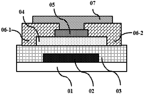
1. A doped metal oxide semiconductor, characterized in that the doped metal oxide semiconductor is a rare-earth oxide doped metal oxide; in which the metal oxide is indium tin oxide having an In:Sn molar ratio of 2:1 to 5:1 or indium tin zinc oxide having molar ratios of In, Sn, and Zn in ranges of: 0.2≤In/(In+Sn+Zn)≤0.8, 0.2≤Sn/(In+Sn+Zn)≤0.4, 0<Zn/(In+Sn+Zn)≤0.5; the rare-earth oxide comprises ytterbium oxide; an uniform doping molar ratios of ytterbium to the indium and tin or indium and tin and zinc of the metal oxide is in a range from 0.1:1 to 0.4:1; there are recombination centers for photo-induced carriers generated in the doped metal oxide semiconductor.