| CPC H01L 29/78621 (2013.01) [H01L 29/42384 (2013.01); H01L 29/66969 (2013.01); H01L 27/1225 (2013.01); H01L 29/4908 (2013.01); H01L 29/7869 (2013.01); H01L 2029/42388 (2013.01)] | 9 Claims |
|
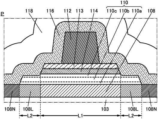
1. A semiconductor device comprising a semiconductor layer, a first insulating layer, a second insulating layer, a metal oxide layer, and a conductive layer,
wherein the first insulating layer, the metal oxide layer, and the conductive layer are stacked in this order over the semiconductor layer,
wherein an end portion of the first insulating layer is located inward from an end portion of the semiconductor layer,
wherein an end portion of the metal oxide layer is located inward from the end portion of the first insulating layer,
wherein an end portion of the conductive layer is located inward from the end portion of the metal oxide layer,
wherein the second insulating layer is provided to cover the semiconductor layer, the first insulating layer, the metal oxide layer, and the conductive layer,
wherein the semiconductor layer comprises a first region, a pair of second regions, and a pair of third regions,
wherein the first region overlaps with the first insulating layer and the metal oxide layer,
wherein the second regions between which the first region is sandwiched overlap with the first insulating layer and do not overlap with the metal oxide layer,
wherein the third regions between which the first region and the pair of second regions are sandwiched do not overlap with the first insulating layer,
wherein the third regions are in contact with the second insulating layer,
wherein the third regions comprise a portion having lower resistance than the first region, and
wherein the second regions comprise a portion having higher resistance than the third regions.
|