US 11,894,465 B2
Deep gate-all-around semiconductor device having germanium or group III-V active layer
Ravi Pillarisetty, Portland, OR (US); Willy Rachmady, Beaverton, OR (US); Van H. Le, Beaverton, OR (US); Seung Hoon Sung, Beaverton, OR (US); Jessica S. Kachian, Portland, OR (US); Jack T. Kavalieros, Portland, OR (US); Han Wui Then, Portland, OR (US); Gilbert Dewey, Hillsboro, OR (US); Marko Radosavljevic, Beaverton, OR (US); Benjamin Chu-Kung, Hillsboro, OR (US); and Niloy Mukherjee, Beaverton, OR (US)
Assigned to Google LLC, Mountain View, CA (US)
Filed by Google LLC, Mountain View, CA (US)
Filed on Feb. 12, 2021, as Appl. No. 17/174,935.
Application 14/821,561 is a division of application No. 13/749,139, filed on Jan. 24, 2013, granted, now 9,136,343, issued on Sep. 15, 2015.
Application 17/174,935 is a continuation of application No. 16/011,308, filed on Jun. 18, 2018, granted, now 10,950,733.
Application 16/011,308 is a continuation of application No. 15/465,448, filed on Mar. 21, 2017, granted, now 10,026,845, issued on Jul. 17, 2018.
Application 15/465,448 is a continuation of application No. 15/134,093, filed on Apr. 20, 2016, granted, now 9,640,671, issued on May 2, 2017.
Application 15/134,093 is a continuation of application No. 14/821,561, filed on Aug. 7, 2015, granted, now 9,337,291, issued on May 10, 2016.
Prior Publication US 2021/0167216 A1, Jun. 3, 2021
This patent is subject to a terminal disclaimer.
Int. Cl. H01L 29/165 (2006.01); H01L 29/205 (2006.01); H01L 29/786 (2006.01); H01L 29/06 (2006.01); H01L 29/78 (2006.01); H01L 29/423 (2006.01); H01L 29/66 (2006.01)
CPC H01L 29/78609 (2013.01) [H01L 29/0653 (2013.01); H01L 29/0673 (2013.01); H01L 29/0676 (2013.01); H01L 29/165 (2013.01); H01L 29/205 (2013.01); H01L 29/42392 (2013.01); H01L 29/66742 (2013.01); H01L 29/785 (2013.01); H01L 29/78606 (2013.01); H01L 29/78618 (2013.01); H01L 29/78681 (2013.01); H01L 29/78684 (2013.01); H01L 29/78696 (2013.01)] 20 Claims
OG exemplary drawing
 
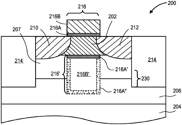
1. A non-planar semiconductor device, comprising:
a hetero-structure disposed above a substrate, the hetero-structure comprising a hetero junction between an upper layer and a lower layer of differing composition;
an active layer disposed above the hetero-structure and having a composition different from the upper and lower layers of the hetero-structure;
a gate structure disposed on and surrounding a channel region of the active layer, and disposed in a trench in the upper layer and at least partially in the lower layer of the hetero-structure;
one or more nanowires disposed in a vertical arrangement above the active layer, wherein the gate structure is disposed on and surrounds each of the nanowires;
source and drain regions disposed on the substrate and in the upper layer on either side of the gate structure; and
isolation regions adjacent the source and drain regions and disposed at least partially into the hetero-structure.