| CPC H01L 29/7853 (2013.01) [H01L 29/0653 (2013.01); H01L 29/0673 (2013.01); H01L 29/0847 (2013.01); H01L 29/42392 (2013.01)] | 20 Claims |
|
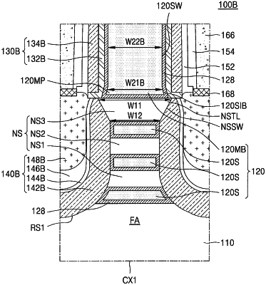
1. A method of manufacturing an integrated circuit, the method comprising:
alternately forming a plurality of semiconductor layers and a plurality of sacrificial layers on a substrate;
patterning the plurality of semiconductor layers and the plurality of sacrificial layers to form a channel stack extending in a first direction;
forming a dummy gate structure on the channel stack, the dummy gate structure including a dummy gate insulating layer pattern and a dummy gate;
forming a spacer structure on a sidewall of the dummy gate structure, the spacer structure including a first spacer layer and a second spacer layer, the first spacer layer including a portion overhanging laterally and outwardly;
forming a plurality of semiconductor patterns and forming a recess region by removing a portion of the channel stack, the portion of the channel stack being not covered by the spacer structure, and an uppermost one of the plurality of semiconductor patterns having an inverted trapezoidal cross-section and an inclined sidewall;
forming a semiconductor layer in the recess region;
forming a gate space by removing the dummy gate structure and the plurality of sacrificial layers, the gate space including sub gate spaces between the plurality of semiconductor patterns; and
forming a gate electrode in the gate space.
|