| CPC H01L 29/78391 (2014.09) [H01L 29/401 (2013.01); H01L 29/516 (2013.01); H01L 29/6684 (2013.01); H01L 29/66545 (2013.01)] | 20 Claims |
|
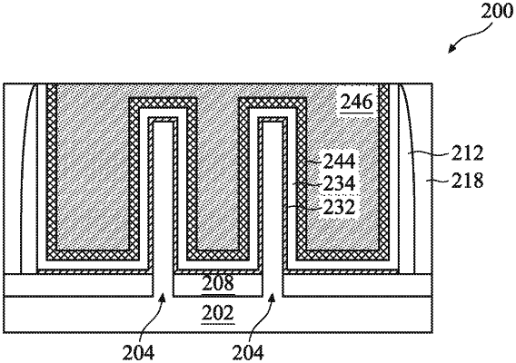
1. A semiconductor device, comprising:
a semiconductor substrate;
a first transistor and a second transistor formed on the semiconductor substrate, each one of the first and second transistors further comprising:
an interfacial layer formed on the semiconductor substrate;
a high-k dielectric layer formed on the interfacial layer; and
a conductive gate electrode layer formed on the high-k dielectric layer,
wherein at least one of the high-k dielectric layer and the interfacial layer is doped with:
a first dopant species with a first concentration,
a second dopant species with a second concentration, and
a third dopant species with a third concentration,
wherein the first dopant species and the second dopant species form a plurality of first dipole elements having a first polarity,
wherein the third dopant species forms a plurality of second dipole elements having a second polarity, and
wherein the first and second polarities are opposite,
wherein the first transistor has a first concentration ratio of the first concentration of the first dopant species to the third concentration of the third dopant species in the at least one of the high-k dielectric layer and the interfacial layer of the first transistor,
wherein the second transistor has a second concentration ratio of first concentration of the first dopant species to the third concentration of the third dopant species in the at least one of the high-k dielectric layer and the interfacial layer of the second transistor, and
wherein the first concentration ratio is different from the second concentration ratio.
|