| CPC H01L 29/78391 (2014.09) [H01L 21/02057 (2013.01); H01L 21/02236 (2013.01); H01L 21/02603 (2013.01); H01L 29/0673 (2013.01); H01L 29/42392 (2013.01); H01L 29/4908 (2013.01); H01L 29/6684 (2013.01); H01L 29/66545 (2013.01); H01L 29/66742 (2013.01); H01L 29/78696 (2013.01)] | 19 Claims |
|
1. A method for forming a semiconductor device structure, comprising:
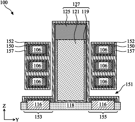
forming a first fin structure and a second fin structure, each first and second fin structure comprises a plurality of first semiconductor layers and a plurality of second semiconductor layers alternatingly stacked;
forming a sacrificial gate structure over the first and second fin structures;
forming a source/drain feature on opposite sides of the sacrificial gate structure, the source/drain feature being in contact with the plurality of first semiconductor layers of the first and second fin structures;
removing the sacrificial gate structure and portions of the plurality of second semiconductor layers to expose portions of each of the plurality of first semiconductor layers of the first and second fin structures;
forming a dipole layer to surround exposed portions of each of the plurality of first semiconductor layers of the first and second fin structures formed as a result of the removal of the sacrificial gate structure and the second semiconductor layers, wherein the dipole layer comprises germanium;
subjecting the dipole layer over the first and second fin structures to a thermal treatment such that portions of germanium in the dipole layer diffuse into and mix with each of the plurality of first and second semiconductor layers of the first and second fin structures to form an intermixed layer, wherein the intermixed layer has a Ge concentration profile gradually and continuously changed along a thickness of the intermixed layer;
forming a capping layer to surround and in contact with the dipole layer, wherein forming a capping layer further comprises:
forming a pure silicon layer on the dipole layer; and
subjecting the pure silicon layer to a wet cleaning process to oxidize a surface portion of the silicon layer;
forming a first interfacial layer to surround the capping layer;
forming a second interfacial layer to surround exposed portions of each of the plurality of first semiconductor layers of the second fin structure; and
forming a gate electrode layer to surround each of the plurality of first semiconductor layers of the first and second fin structures.
|