| CPC H01L 29/7835 (2013.01) [H01L 29/401 (2013.01); H01L 29/402 (2013.01); H01L 29/4916 (2013.01); H01L 29/4966 (2013.01); H01L 29/4991 (2013.01); H01L 29/66484 (2013.01); H01L 29/66545 (2013.01); H01L 29/66553 (2013.01); H01L 29/66659 (2013.01); H01L 29/7831 (2013.01)] | 20 Claims |
|
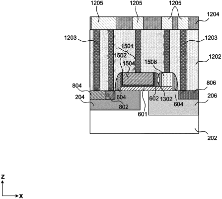
1. A method for forming a semiconductor structure, the method comprising:
forming a channel region and a drift region in a substrate, wherein the channel region and the drift region are non-overlapping with each other;
depositing a gate dielectric layer directly on top surfaces of the channel region, the drift region, and a portion of the substrate between the channel region and the drift region;
depositing a gate material on the gate dielectric layer;
etching the gate material to form a dual gate structure comprising:
a first gate structure over the channel and drift regions; and
a second gate structure over the drift region;
etching the gate dielectric layer to form:
a continuous layer under the first and second gate structures,
a first sidewall of the gate dielectric layer aligned with an outer sidewall of the first gate structure, and
a second sidewall of the gate dielectric layer aligned with an outer sidewall of the second gate structure, wherein the outer sidewalls of the first and second gate structures face opposite to each other;
forming a first outer spacer on a first outer sidewall of the first gate structure and in physical contact with the top surface of the channel region;
forming a second outer spacer on a second outer sidewall of the second gate structure and in physical contact with the top surface of the drift region;
forming an inner spacer in contact with the first and second gate structures;
etching the first gate structure to expose a top surface of the gate dielectric layer; and
forming a metal gate structure with a bottom surface directly on the top surface of the gate dielectric layer and with a sidewall in physical contact with the first outer spacer.
|