| CPC H01L 29/7825 (2013.01) | 15 Claims |
|
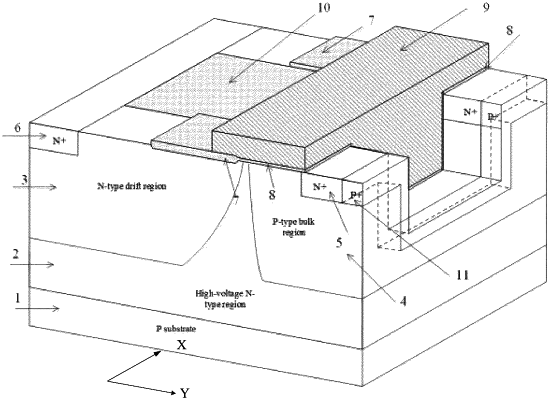
1. A lateral double-diffused metal oxide semiconductor field effect transistor, comprising:
a source region of a first conductivity type;
a drain region of the first conductivity type;
a drift region of the first conductivity type;
a bulk region of a second conductivity type;
a field oxide layer located on a surface of the drift region;
a trench gate comprising a lower part inside a trench and an upper part outside the trench, a length of the lower part in a width direction of a conducting channel being less than that of the upper part in the width direction of the conducting channel, and the lower part extending into the bulk region and having a depth less than that of the bulk region; and
an insulation structure arranged between the drain region and the trench gate and extending downwards into the drift region, a depth of the insulation structure being less than that of the drift region, a depth of the insulation structure in the drift region being greater than that of the field oxide layer in the drift region, a length of the insulation structure in the width direction of the conducting channel being less than that of the drift region in the width direction of the conducting channel, the field oxide layers being formed on surfaces of two sides of the insulation structure in the width direction of the conducting channel, and the upper part extending onto the field oxide layer; the first conductivity type and the second conductivity type being opposite conductivity types.
|