| CPC H01L 29/7786 (2013.01) [H01L 21/2233 (2013.01); H01L 21/2236 (2013.01); H01L 21/3065 (2013.01); H01L 29/2003 (2013.01); H01L 29/205 (2013.01); H01L 29/207 (2013.01); H01L 29/4236 (2013.01); H01L 29/513 (2013.01); H01L 29/66462 (2013.01)] | 12 Claims |
|
1. A semiconductor device comprising:
a nitride semiconductor layer;
a silicon oxide layer; and
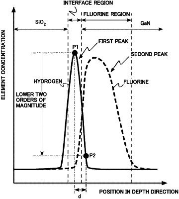
a first region disposed between the nitride semiconductor layer and the silicon oxide layer and containing at least one element of hydrogen and deuterium,
wherein in a concentration distribution of the at least one element in the silicon oxide layer, the first region, and the nitride semiconductor layer, a distance between a first position at which a concentration of the at least one element has a maximum value and a second position present on the side of the nitride semiconductor layer with respect to the first position and having the concentration of the at least one element which is two orders of magnitude lower than the maximum value is 1 nm or less.
|