US 11,894,443 B2
Method of making gate structure of a semiconductor device
Ming Zhu, Hsinchu (TW); Hui-Wen Lin, Hsinchu (TW); Harry Hak-Lay Chuang, Hsinchu (TW); Bao-Ru Young, Hsinchu (TW); Yuan-Sheng Huang, Hsinchu (TW); Ryan Chia-Jen Chen, Hsinchu (TW); Chao-Cheng Chen, Hsinchu (TW); Kuo-Cheng Ching, Hsinchu (TW); Ting-Hua Hsieh, Hsinchu (TW); and Carlos H. Diaz, Hsinchu (TW)
Assigned to TAIWAN SEMICONDUCTOR MANUFACTURING COMPANY, LTD., Hsinchu (TW)
Filed by TAIWAN SEMICONDUCTOR MANUFACTURING COMPANY, LTD., Hsinchu (TW)
Filed on Jun. 16, 2022, as Appl. No. 17/842,718.
Application 17/842,718 is a division of application No. 16/779,356, filed on Jan. 31, 2020, granted, now 11,380,775.
Application 15/456,889 is a division of application No. 13/277,642, filed on Oct. 20, 2011, granted, now 9,595,443, issued on Mar. 14, 2017.
Application 16/779,356 is a continuation of application No. 15/984,720, filed on May 21, 2018, granted, now 10,553,699, issued on Feb. 4, 2020.
Application 15/984,720 is a continuation of application No. 15/456,889, filed on Mar. 13, 2017, granted, now 9,978,853, issued on May 22, 2018.
Prior Publication US 2022/0320314 A1, Oct. 6, 2022
Int. Cl. H01L 29/66 (2006.01); H01L 21/8234 (2006.01); H01L 29/423 (2006.01); H01L 29/49 (2006.01); H01L 21/28 (2006.01)
CPC H01L 29/66545 (2013.01) [H01L 21/28088 (2013.01); H01L 21/82345 (2013.01); H01L 21/823437 (2013.01); H01L 21/823475 (2013.01); H01L 21/823481 (2013.01); H01L 29/42376 (2013.01); H01L 29/4966 (2013.01)] 20 Claims
OG exemplary drawing
 
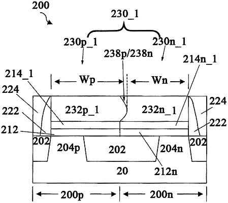
1. A method of making a semiconductor device comprising:
depositing a TiN layer over a substrate;
doping a first portion of the TiN layer using an oxygen-containing plasma treatment;
doping a second portion of the TiN layer using a nitrogen-containing plasma treatment, wherein the second portion of the TiN layer directly contacts the first portion of the TiN layer;
forming a first metal gate electrode over the first portion of the TiN layer; and
forming a second metal gate electrode over the second portion of the TiN layer, wherein the first metal gate electrode has a different work function from the second metal gate electrode, the second metal gate electrode directly contacts the first metal gate electrode, a top-most surface of the first metal gate electrode is co-planar with a top-most surface of the second metal gate electrode, and at least one of the first metal gate electrode or the second metal gate electrode has a variable width in a direction parallel to a top surface of the substrate.