| CPC H01L 29/6653 (2013.01) [H01L 29/0653 (2013.01); H01L 29/66545 (2013.01); H01L 29/66553 (2013.01); H01L 29/66742 (2013.01); H01L 29/78696 (2013.01); H01L 29/0665 (2013.01); H01L 29/42392 (2013.01)] | 20 Claims |
|
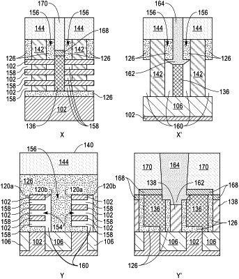
1. A nanosheet transistor for reducing parasitic capacitance, comprising:
a spacer region between a high-k metal gate and an epitaxial layer, wherein the spacer region comprises:
a first nanosheet stack comprising a first nanosheet and a second nanosheet;
an inner spacer region between the first nanosheet and the second nanosheet; and
a side subway region located along an edge of the first nanosheet, the inner spacer region, and the second nanosheet, wherein the side subway region contacts a shallow trench isolation below the spacer region.
|