| CPC H01L 29/4983 (2013.01) [H01L 29/4238 (2013.01); H01L 29/7835 (2013.01); H01L 21/26513 (2013.01)] | 6 Claims |
|
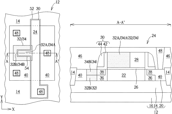
1. A semiconductor device, comprising:
a gate structure on a substrate, wherein the gate structure comprises:
a main branch extending along a first direction on the substrate; and
a sub-branch extending along a second direction adjacent to the main branch;
a first doped region having dopants of a first conductive type disposed in an entire electrode of the sub-branch and in an adjacent part of an electrode of the main branch, comprises a higher concentration of the first conductive type dopants than a remaining part of the first conductive doped main branch electrode;
a second doped region having dopants of the first conductive type disposed in the substrate and disposed adjacent to the sub-branch of the gate structure;
a source/drain region adjacent to two sides of the gate structure;
a plurality of contact plugs disposed on the source/drain region, wherein the first doped region and the second doped region do not overlap with the contact plugs;
a spacer disposed on the substrate and surrounding the gate structure; and
a lightly doped drain region disposed in the substrate and disposed under the spacer.
|