| CPC H01L 29/45 (2013.01) [H01L 21/7684 (2013.01); H01L 21/76805 (2013.01); H01L 21/76843 (2013.01); H01L 21/76882 (2013.01); H01L 21/76895 (2013.01); H01L 23/535 (2013.01); H01L 23/53209 (2013.01); H01L 29/7851 (2013.01)] | 20 Claims |
|
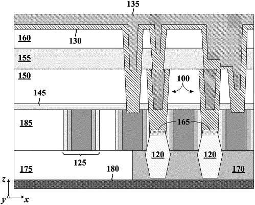
1. A structure, comprising:
a substrate with a gate structure and a source/drain (S/D) structure disposed thereon;
a bottom dielectric surrounding a lower portion of the gate structure and the S/D structure;
an etch stop layer on the bottom dielectric;
a first dielectric on the gate and S/D structures;
a second dielectric on the first dielectric; and
a shared conductive structure in the first dielectric contacting the gate structure and the S/D structure, wherein the shared conductive structure comprises:
a ruthenium liner on a bottom surface and sidewall surfaces of the shared conductive structure and contacting the first dielectric and etch stop layer;
a first thickness of the ruthenium liner on the bottom surface contacting the S/D structure and a second thickness of the ruthenium liner on the bottom surface contacting the first dielectric between the S/D structure and the gate structure, wherein the first thickness is greater than the second thickness; and
a cobalt metal in contact with the ruthenium liner.
|
|
9. A structure, comprising:
a substrate with gate structures and source/drain (S/D) structures disposed thereon;
first conductive structures extending through a first dielectric layer and disposed on the S/D structures;
second conductive structures extending through a first dielectric layer and a second dielectric layer and on the gate structures; and
a third conductive structure on a first conductive structure of the first conductive structures, wherein each of the first conductive structures, the second conductive structures, and the third conductive structure comprises:
a ruthenium liner in contact with one or more of the first dielectric layer and the second dielectric layer; and
a cobalt metal in contact with the ruthenium liner.
|
|
16. A structure, comprising:
a substrate with gate structures and source/drain (S/D) structures disposed thereon;
a first dielectric layer comprising a lower conductive structure comprising a ruthenium liner and a cobalt fill, wherein the cobalt fill contacts the ruthenium liner, wherein the ruthenium liner contacts the first dielectric layer, and wherein the lower conductive structure contacts the source/drain (S/D) structures; and
a second dielectric layer comprising a gate conductive structure comprising a ruthenium fill, wherein the gate conductive structure contacts the gate structure, wherein the ruthenium fill contacts the second dielectric layer, and wherein an upper conductive structure contacts the gate conductive structure.
|