| CPC H01L 29/41791 (2013.01) [H01L 21/76832 (2013.01); H01L 21/76897 (2013.01); H01L 23/535 (2013.01); H01L 29/401 (2013.01); H01L 29/7851 (2013.01)] | 20 Claims |
|
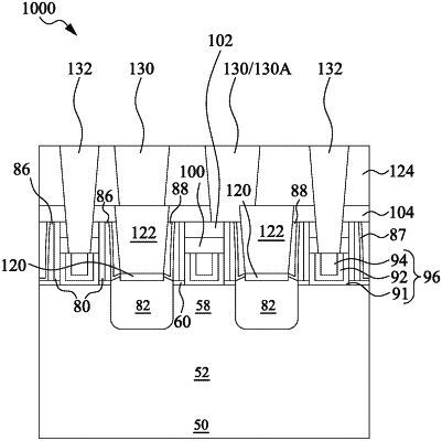
1. A method comprising:
forming a gate stack over a substrate;
recessing the gate stack to form a first recess;
forming a cap layer over the gate stack in the first recess, the cap layer comprising a first material over the gate stack and a second material over the first material, the second material being different from the first material, wherein forming the cap layer comprises:
filling the first recess with the first material; and
performing an oxygen addition process on an upper portion of the first material, the oxygen addition process converting the upper portion of the first material into the second material;
forming a first conductive feature adjacent the gate stack; and
forming a second conductive feature over the first conductive feature, the second conductive feature being in physical contact with a topmost surface of the cap layer and a topmost surface of the first conductive feature.
|