| CPC H01L 29/41733 (2013.01) [H01L 29/0665 (2013.01); H01L 29/401 (2013.01); H01L 29/42392 (2013.01)] | 16 Claims |
|
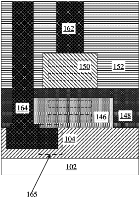
1. A stacked semiconductor device comprising:
a lower source/drain epi located on top of a bottom dielectric layer;
an isolation layer located on top of the lower source/drain epi;
an upper source/drain epi located on top of the isolation layer; and
a lower electrical contact that is connected to the lower source/drain epi, wherein the lower electrical contact is in direct contact with multiple side surfaces of the lower source/drain epi, wherein the lower electrical contact extends under the lower source/drain epi.
|