| CPC H01L 29/41708 (2013.01) [H01L 29/401 (2013.01); H01L 29/456 (2013.01); H01L 29/66333 (2013.01); H01L 29/7395 (2013.01)] | 20 Claims |
|
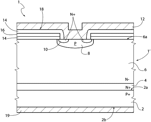
1. A vertical-conduction semiconductor device, comprising:
a silicon substrate having a front face and a rear face;
a front-side structure on the front face of the silicon substrate, the front-side structure having at least one current-conduction region at a respective front face; and
a back side metal structure on the rear face of the silicon substrate, in electrical contact with the silicon substrate, and including an overlapped stack of metal layers,
the back side metal structure including:
a first metal layer including nickel and vanadium;
a silicide region between the rear face of the silicon substrate and the first metal layer, and in electrical contact with the rear face of the silicon substrate, the silicide region including nickel silicide;
an interface region between the first metal layer and the silicide region, the interface region including nitrogen and vanadium; and
a second metal layer on the first metal layer.
|