| CPC H01L 29/408 (2013.01) [H10B 43/27 (2023.02)] | 16 Claims |
|
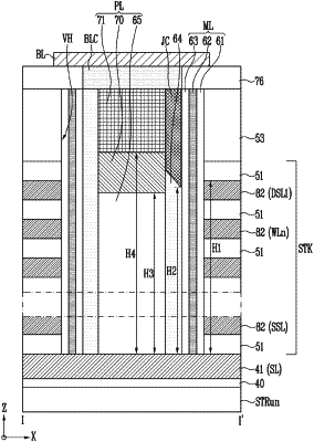
1. A memory device comprising:
a stack structure including word lines and a select line;
a vertical hole vertically penetrating the stack structure; and
a memory layer, a channel layer, and a plug, sequentially formed along an inner side surface of the vertical hole,
wherein the plug includes a material layer having a fixed negative charge, and
wherein a bottom surface of the material layer is located between a bottom surface and a top surface of the select line.
|