| CPC H01L 29/404 (2013.01) [H01L 29/0607 (2013.01); H01L 29/1095 (2013.01)] | 16 Claims |
|
1. A semiconductor structure, comprising:
a substrate;
a first well, disposed in the substrate and having a first conductivity type;
a second well, disposed in the substrate, adjacent to the first well, and having a second conductivity type that is opposite to the first conductivity type;
a first doped region, disposed in the first well;
a second doped region, disposed in the second well;
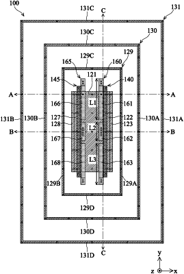
a first gate structure and a second gate structure, the first gate structure is disposed between the first doped region and the second doped region;
a first insulating layer, overlapping a portion of the first well and a portion of the first gate structure; and
a first field plate structure, disposed on the first insulating layer and at least partially overlapping the first gate structure, wherein the first field plate structure is segmented into a first partial field plate having a first length, a second partial field plate having a second length, and a third partial field plate having a third length along a first direction, wherein the first gate structure and the second gate structure are arranged along a second direction perpendicular to the first direction, wherein the first partial field plate, the second partial field plate and the third partial field plate are separated from each other, and wherein the first length and the third length are greater than the second length.
|