| CPC H01L 29/1608 (2013.01) [H01L 29/872 (2013.01)] | 16 Claims |
|
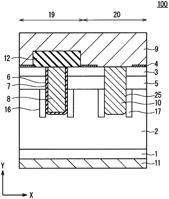
1. A silicon carbide semiconductor device that includes a Schottky barrier diode in a field-effect transistor, the silicon carbide semiconductor device comprising:
a semiconductor layer of a first conductivity type;
a first semiconductor region of the first conductivity type provided in an upper layer portion of the semiconductor layer;
a second semiconductor region of a second conductivity type provided in contact with a bottom face of the first semiconductor region;
a first trench provided through the first semiconductor region and the second semiconductor region in a thickness direction and having a bottom face that reaches inside the semiconductor layer;
a gate electrode embedded in the first trench via a gate insulating film that covers an inner face of the first trench;
an interlayer insulation film having a contact portion above the first semiconductor region;
a first low-resistance layer of the first conductivity type provided in the semiconductor layer to have contact with at least one trench side wall of the first trench in a direction perpendicular to a direction of extension of the first trench;
a second trench provided through the second semiconductor region in the thickness direction and having a bottom face that reaches inside the semiconductor layer;
a Schottky barrier diode electrode embedded in the second trench;
a second low-resistance layer of the first conductivity type provided in the semiconductor layer to have contact with at least one trench side wall of the second trench in a direction perpendicular to a direction parallel to a direction of extension of the second trench;
a first main electrode embedded in the contact portion and covering the interlayer insulation film; and
a second main electrode provided on a main surface of the semiconductor layer on a side opposite to a side on which the first main electrode is provided,
wherein the second low-resistance layer has an impurity concentration higher than an impurity concentration in the semiconductor layer and lower than an impurity concentration in the first low-resistance layer.
|