| CPC H01L 29/0673 (2013.01) [H01L 21/02532 (2013.01); H01L 21/02603 (2013.01); H01L 21/823412 (2013.01); H01L 21/823418 (2013.01); H01L 21/823431 (2013.01); H01L 21/823437 (2013.01); H01L 21/823468 (2013.01); H01L 27/0886 (2013.01); H01L 29/0847 (2013.01); H01L 29/165 (2013.01); H01L 29/6656 (2013.01); H01L 29/6681 (2013.01); H01L 29/66545 (2013.01); H01L 29/66553 (2013.01); H01L 29/7851 (2013.01)] | 20 Claims |
|
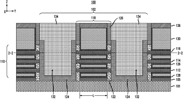
1. A semiconductor device, comprising:
a nanosheet field-effect transistor device disposed on a semiconductor substrate, wherein the nano sheet field-effect transistor device comprises:
a plurality of nanosheet stack structures each comprising a plurality of semiconductor channel layers;
a gate structure on the nanosheet stack structures;
a gate sidewall spacer on the gate structure;
a source/drain region in contact with sidewalls of the nanosheet stack structures and on a portion of the gate sidewall spacer to define a trench between opposing sidewalls; and
a metal-based material disposed in the trench, on a top surface of the source/drain region and on the gate sidewall spacer;
wherein the source/drain region is disposed on the sidewalls of the nanosheet stack structures and on a portion of an oxide layer disposed over a portion of the semiconductor substrate;
wherein the source/drain region has a uniform thickness along the sidewalls of the nanosheet stack structures and on the portion of the gate sidewall spacer; and
wherein the trench extends through the source/drain region to the oxide layer.
|