| CPC H01L 29/0653 (2013.01) [H01L 21/02057 (2013.01); H01L 21/02227 (2013.01); H01L 21/30604 (2013.01); H01L 29/0847 (2013.01); H01L 29/66636 (2013.01); H01L 29/66795 (2013.01); H01L 29/7848 (2013.01); H01L 29/7851 (2013.01); H01L 21/3065 (2013.01)] | 20 Claims |
|
1. A device comprising:
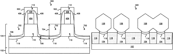
a first protrusion disposed on a substrate, the first protrusion formed of a semiconductor material;
a first silicon-containing channel region disposed on a first portion of the first protrusion
a first gate structure wrapping around the first silicon-containing channel region;
a first source/drain feature disposed on a second portion the first protrusion; and
a second silicon-containing channel region disposed on a third portion of the first protrusion;
a second gate structure wrapping around the second silicon-containing channel region;
a first electrical barrier layer disposed under and interfacing with the first source/drain feature, the first silicon-containing channel region and the second silicon-containing channel region such that the first electrical barrier layer extends continuously from first silicon-containing channel region to the second silicon-containing channel region.
|