| CPC H01L 28/91 (2013.01) [H01L 28/87 (2013.01); H01L 28/88 (2013.01); H01L 28/92 (2013.01); H10B 12/00 (2023.02)] | 18 Claims |
|
1. A fabrication method for a double-sided capacitor, comprising the following steps:
providing a substrate, wherein a capacitor contact pad is formed on a surface of the substrate;
forming a stack structure on the substrate to cover the capacitor contact pad;
forming a capacitor hole in a direction perpendicular to the substrate to penetrate the stack structure and expose the capacitor contact pad, wherein the stack structure comprises sacrificial layers and supporting layers alternately stacked;
forming an auxiliary layer to cover a sidewall of the capacitor hole;
forming a first electrode layer to cover a surface of the auxiliary layer and the exposed capacitor contact pad;
removing a part of the supporting layer on a top of the stack structure to form an opening to expose the sacrificial layers;
removing the sacrificial layers and the auxiliary layer simultaneously along the opening to form a gap between the supporting layers and the first electrode layer; and
forming a dielectric layer covering a surface of the first electrode layer and a second electrode layer covering a surface of the dielectric layer, wherein the gap is at least filled with the dielectric layer.
|
|
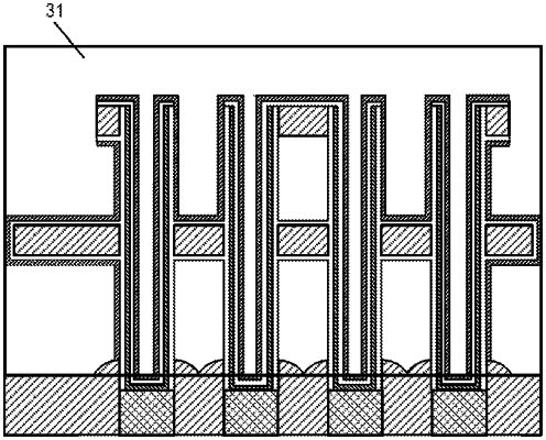
12. A double-sided capacitor, comprising:
a substrate, having a capacitor contact pad on its surface;
a top supporting layer and a middle supporting layer, each of which is provided with a number of capacitor pores, and on a plane parallel to the substrate, a projection area of the middle supporting layer is greater than that of the top supporting layer, wherein the middle supporting layer is opened only at the capacitor pores, and a projection of the capacitor pores on the substrate overlaps with the capacitor contact pad;
a first electrode layer, being of a shape of a hollow column with an opening in the top, wherein the first electrode layer is perpendicular to the surface of the substrate and penetrates the top supporting layer and the middle supporting layer through the capacitor pores, wherein the bottom of the first electrode layer is in contact with the capacitor contact pad;
a dielectric layer, covering the surfaces of the first electrode layer, the top supporting layer and the middle supporting layer; and
a second electrode layer, covering the surface of the dielectric layer.
|