| CPC H01L 28/91 (2013.01) [H01L 28/87 (2013.01); H10B 12/31 (2023.02)] | 19 Claims |
|
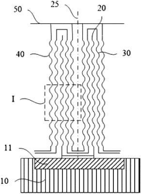
1. A semiconductor structure, comprising:
a substrate, comprising an active area;
a first electrode layer, arranged on the substrate and electrically connected to the active area, the first electrode layer extending in a direction perpendicular to the substrate;
a dielectric layer, arranged on a surface of the first electrode layer; and
a second electrode layer, arranged on a surface of the dielectric layer,
wherein each of the surface of the first electrode layer and the surface of the dielectric layer is provided an uneven structure,
wherein a projection of the first electrode layer on the substrate is a first ring, and a projection of the dielectric layer on the substrate comprises a second ring and a third ring, the second ring being nested inside the first ring, and the third ring being sleeved outside the first ring; and
wherein a projection of the second electrode layer on the substrate comprises a solid portion and a fourth ring, the solid portion being located inside the second ring, and the fourth ring being sleeved outside the third ring.
|