| CPC H01L 28/57 (2013.01) [H01L 21/324 (2013.01); H01L 21/76832 (2013.01); H01L 28/65 (2013.01); H01L 28/75 (2013.01); H10B 53/30 (2023.02); H10N 70/8836 (2023.02)] | 20 Claims |
|
1. A method of fabricating a device structure, the method comprising:
forming an electrode structure in a memory region by a first process comprising:
etching a first opening in an etch stop layer and exposing a conductive interconnect below the etch stop layer;
depositing a first conductive material on the conductive interconnect; and
depositing a first conductive hydrogen barrier layer in the first conductive material; and
depositing a dielectric on the etch stop layer;
forming a trench capacitor by a second process comprising:
forming a trench in the dielectric, the trench exposing at least a portion of the electrode structure;
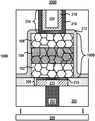
depositing a first electrode layer on a base and on sidewalls of the trench, wherein the first electrode layer comprises a first conductive nonlinear polar material, the first conductive nonlinear polar material comprising a first grain length;
depositing a dielectric layer comprising a perovskite material on the first electrode layer, the perovskite material comprising a second grain length;
depositing a second electrode layer on the dielectric layer, wherein the second electrode layer comprises a second conductive nonlinear polar material, the second conductive nonlinear polar material comprising a third grain length that is substantially equal to the first grain length; and
performing a post deposition anneal (PDA) for a duration of less than 60 seconds at temperatures below 1300 degrees Celsius, wherein the PDA modifies the first conductive nonlinear polar material to have a first new grain length which is a factor of 3 larger than the first grain length, wherein the PDA modifies the perovskite material to have a second new grain length which is a factor of 3 larger than the second grain length, and wherein the PDA modifies the second conductive nonlinear polar material to have a third new grain length which is a factor of 3 larger than the third grain length; and
forming a via electrode on the trench capacitor by a third process comprising:
depositing a second conductive hydrogen barrier layer on the second electrode layer; and
depositing a second conductive material on the second conductive hydrogen barrier layer.
|
|
14. A method of fabricating a device structure, the method comprising:
fabricating a transistor, the method comprising:
forming a fin structure in a substrate by patterning the substrate;
forming an isolation adjacent to the fin structure;
forming an epitaxial source structure, an epitaxial drain structure and a channel in the fin structure;
performing an activation anneal at a temperature of at least 600 degrees Celsius;
forming a gate on the channel; and
forming a first contact on the epitaxial drain structure and a second contact on the gate;
forming a conductive interconnect on the first contact or on the second contact;
forming an electrode structure by a first process comprising:
etching a first opening in an etch stop layer and exposing at least a portion of the conductive interconnect;
depositing a first conductive hydrogen barrier layer in the first opening;
depositing a first conductive material on the first conductive hydrogen barrier layer; and
depositing a dielectric on the etch stop layer;
forming a trench capacitor by a second process comprising:
forming a trench in the dielectric, the trench exposing at least a portion of the electrode structure;
depositing a first electrode layer on a base and on sidewalls of the trench, wherein the first electrode layer comprises a first conductive nonlinear polar material, the first conductive nonlinear polar material comprising a first grain length;
depositing a dielectric layer comprising a perovskite material on the first electrode layer, the perovskite material comprising a second grain length;
depositing a second electrode layer on the dielectric layer, wherein the second electrode layer comprises a second conductive nonlinear polar material, the second conductive nonlinear polar material comprising a third grain length that is substantially equal to the first grain length; and
performing a post deposition anneal (PDA) for a duration of less than 60 seconds at temperatures below 1300 degree Celsius, wherein the PDA modifies the first conductive nonlinear polar material to have a first new grain length which is a factor of 3 larger than the first grain length, wherein the PDA modifies the perovskite material to have a second new grain length which is a factor of 3 larger than the second grain length, and wherein the PDA modifies the second conductive nonlinear polar material to have a third new grain length which is a factor of 3 larger than the third grain length; and
forming a via electrode on the trench capacitor by a third process comprising:
depositing a second conductive hydrogen barrier layer on the second electrode layer; and
depositing a second conductive material on the second conductive hydrogen barrier layer.
|
|
19. A method of fabricating a device structure, the method comprising:
fabricating a transistor, the method comprising:
forming a fin structure in a substrate by patterning the substrate;
forming an isolation adjacent to the fin structure;
forming an epitaxial source structure, an epitaxial drain structure and a channel in the fin structure;
performing an activation anneal at a temperature of at least 600 degrees Celsius;
forming a gate on the channel; and
forming a first contact on the epitaxial drain structure and a second contact on the gate;
forming a conductive interconnect on the first contact or on the second contact;
forming an electrode structure by a first process comprising:
etching a first opening in an etch stop layer and exposing at least a portion of the conductive interconnect;
depositing a first conductive hydrogen barrier layer in the first opening;
depositing a first conductive material on the first conductive hydrogen barrier layer; and
depositing a dielectric on the etch stop layer;
forming a trench capacitor by a second process comprising:
forming a trench in the dielectric, the trench exposing at least a portion of the electrode structure;
depositing a first electrode layer on a base and on sidewalls of the trench, wherein the first electrode layer comprises a first conductive nonlinear polar material, the first conductive nonlinear polar material comprising a first grain length;
depositing a dielectric layer comprising a perovskite material on the first electrode layer, the perovskite material comprising a second grain length;
performing a post deposition anneal (PDA) for a duration of less than 60 seconds at temperatures below 1300 degree Celsius, wherein the PDA modifies the first conductive nonlinear polar material to have a first new grain length which is a factor of 3 larger than the first grain length, wherein the PDA modifies the perovskite material to have a second new grain length which is a factor of 3 larger than the second grain length; and
depositing a second electrode layer on the dielectric layer, wherein the second electrode layer comprises a second conductive nonlinear polar material, the second conductive nonlinear polar material comprising a third grain length that is less the first grain length; and
forming a via electrode on the trench capacitor by a third process comprising:
depositing a second conductive hydrogen barrier layer on the second electrode layer; and
depositing a second conductive material on the second conductive hydrogen barrier layer.
|