| CPC H01L 27/156 (2013.01) [H01L 25/00 (2013.01)] | 23 Claims |
|
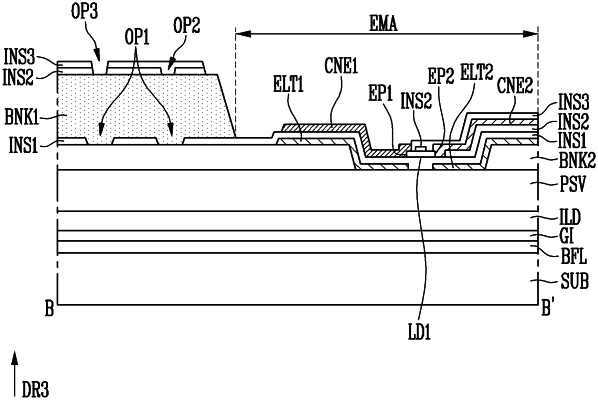
1. A display device comprising:
a substrate including pixels;
a first bank that defines an emission area of the pixels;
a first electrode and a second electrode spaced apart from each other in the emission area;
a first insulating layer disposed on the first electrode and the second electrode;
light emitting elements disposed on the first insulating layer between the first electrode and the second electrode;
a second insulating layer disposed on the first bank;
a first opening passing through the first insulating layer; and
a second opening passing through the second insulating layer, wherein
the first opening and the second opening overlap the first bank, and
an end of each of the light emitting elements is electrically connected to one of the first and second electrodes and another end of each of the light emitting elements is electrically connected to the other one of the first and second electrodes such that the light emitting elements emit light in case that a difference in potential between the first and second electrodes is equal to or greater than a threshold voltage.
|