| CPC H01L 27/1464 (2013.01) [H01L 27/1469 (2013.01); H01L 27/14634 (2013.01); H01L 27/14636 (2013.01)] | 20 Claims |
|
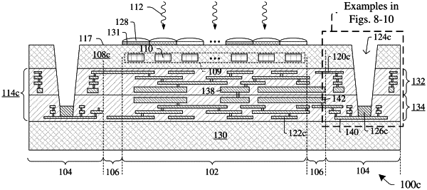
1. An integrated circuit (IC), comprising:
a first substrate including a plurality of imaging devices;
a second substrate disposed under the first substrate and including a plurality of logic devices;
a first interconnect structure disposed between the first substrate and the second substrate and configured to electrically couple imaging devices within the first substrate to one another;
a second interconnect structure disposed between the first interconnect structure and the second substrate, the second interconnect structure configured to electrically couple logic devices within the second substrate to one another;
a bond pad structure coupled to a metal layer of the second interconnect structure and extending along inner sidewalls of both the first interconnect structure and the second interconnect structure; and
an oxide layer extending from above the first substrate to below a plurality of metal layers of the first interconnect structure, and lining inner sidewalls of the bond pad structure.
|