US 11,894,409 B2
Back side illumination image sensors and electronic device including the same
Yun Ki Lee, Hwaseong-si (KR); Jong Hoon Park, Hwaseong-si (KR); and Jun Sung Park, Hwaseong-si (KR)
Assigned to Samsung Electronics Co., Ltd., Gyeonggi-do (KR)
Filed by Samsung Electronics Co., Ltd., Suwon-si (KR)
Filed on Aug. 23, 2021, as Appl. No. 17/409,048.
Application 17/409,048 is a continuation of application No. 16/775,481, filed on Jan. 29, 2020, granted, now 11,101,314, issued on Aug. 24, 2021.
Application 16/775,481 is a continuation of application No. 16/451,561, filed on Jun. 25, 2019, granted, now 11,121,167.
Claims priority of application No. 10-2018-0167379 (KR), filed on Dec. 21, 2018.
Prior Publication US 2021/0384234 A1, Dec. 9, 2021
Int. Cl. H01L 27/146 (2006.01); H10K 59/13 (2023.01)
CPC H01L 27/1464 (2013.01) [H01L 27/1461 (2013.01); H01L 27/1463 (2013.01); H01L 27/14612 (2013.01); H01L 27/14621 (2013.01); H01L 27/14623 (2013.01); H01L 27/14645 (2013.01); H10K 59/13 (2023.02)] 20 Claims
OG exemplary drawing
 
1. An image sensor comprising:
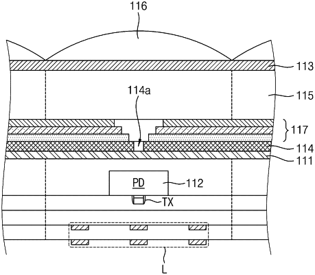
a substrate;
a photodiode in the substrate;
a light shield grid on the photodiode;
a light shielding filter layer formed above the light shield grid, the light shielding filter layer including an opening above the photodiode;
a planarization layer formed above the light shielding filter layer; and
an anti-reflection film, including a plurality of sub-films on and planar to the planarization layer;
wherein the plurality of sub-films comprises a stack including at least a first sub-film and a second sub-film.